Capability across the chip lifecycle.
A six‑stage technical workflow turns an application target into a characterized device and a repeatable production baseline.
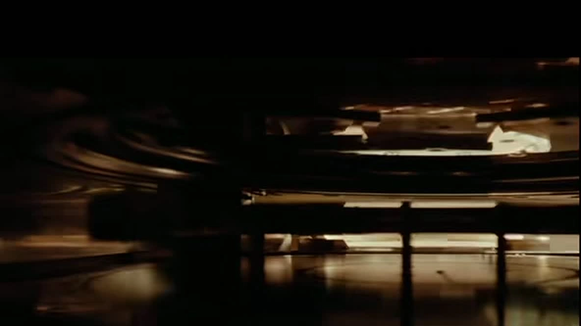
Wafer fabrication
Controlled wafer processing builds the semiconductor structure and prepares each lot for downstream inspection.
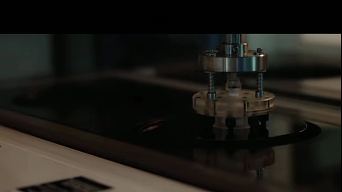
Metallization & dry etching
Electroplating, metal coating and dry etching define contacts, isolation and device geometry.
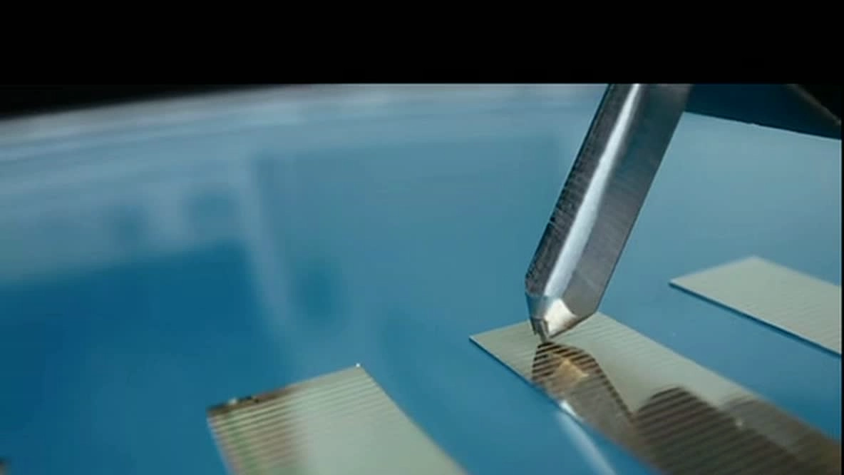
Chip cleaving
Precision cleaving separates laser bars and establishes the optical cavity and facet geometry.
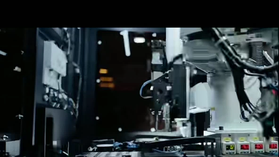
Automated packaging
Die placement and package assembly turn qualified chips into integration‑ready devices.
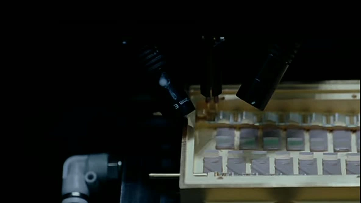
Fiber coupling
Active optical alignment couples the laser output into fiber with controlled efficiency and stability.
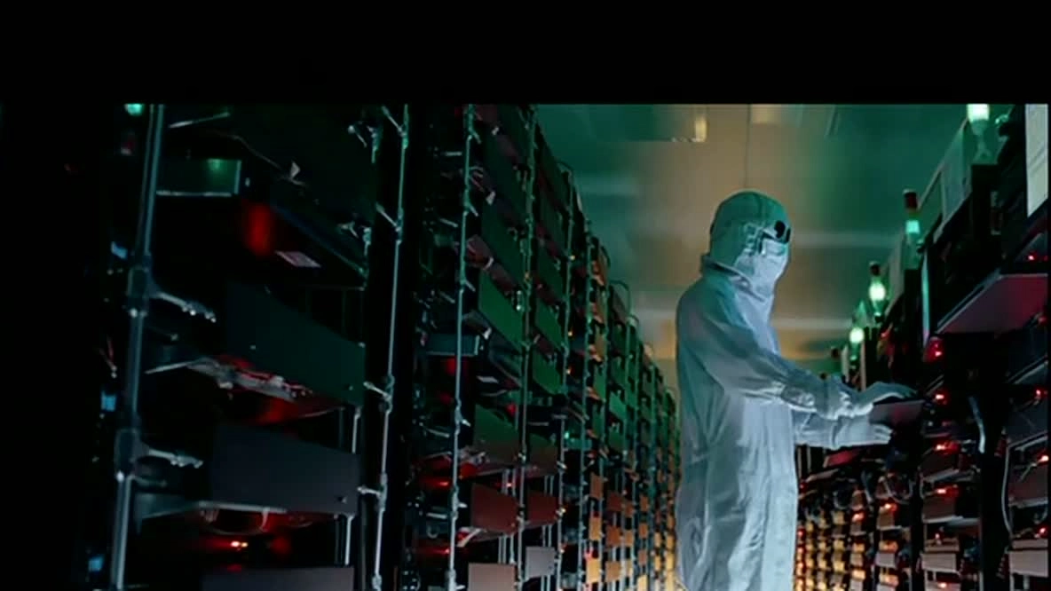
Optical test & burn‑in
Performance screening and accelerated aging verify output, stability and lifetime before release.
A wavelength for every optical challenge.
Current confirmed product wavelengths span visible, near‑infrared and extended infrared. Select a platform by wavelength, application and power requirement.
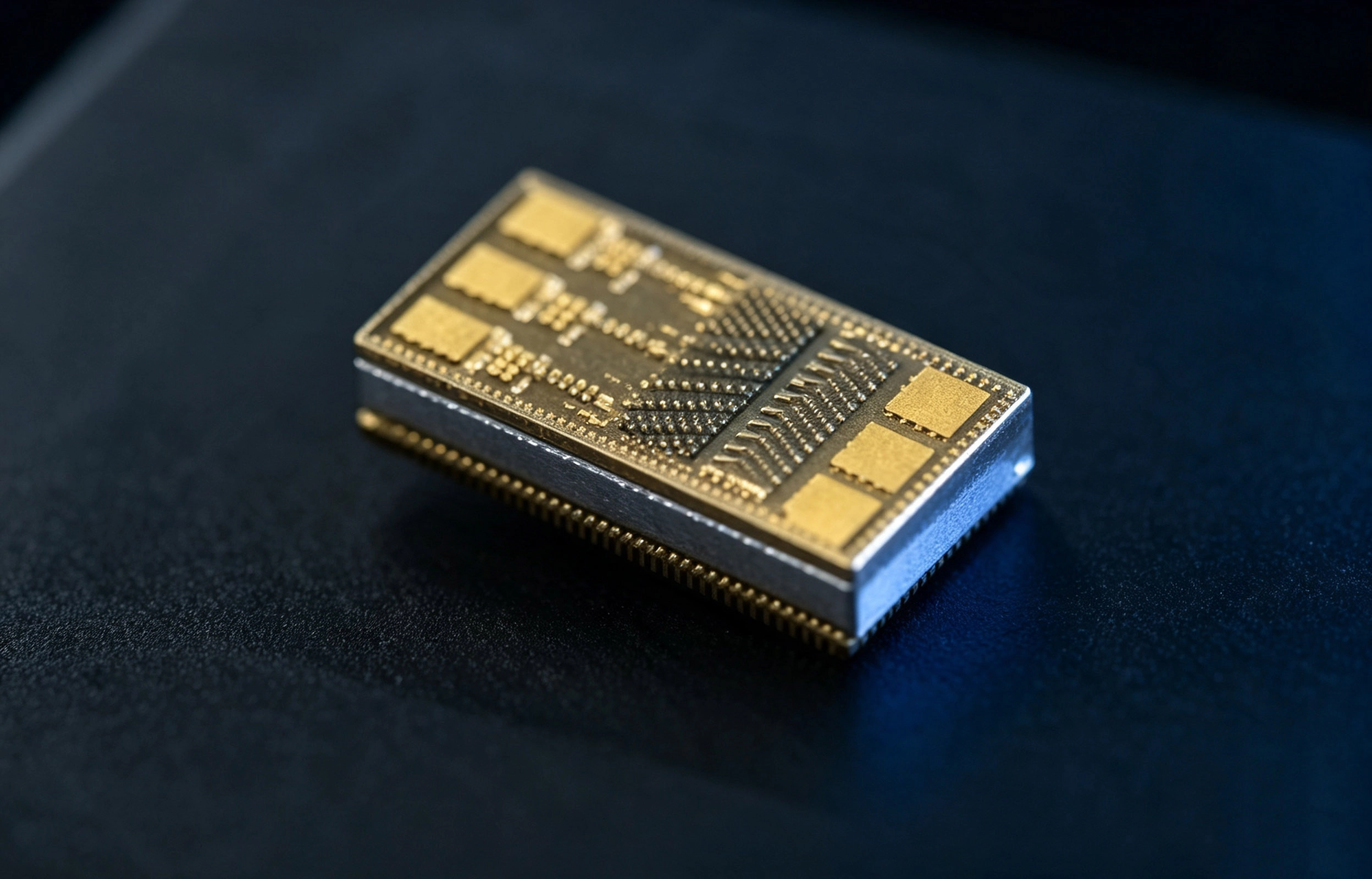
Need a wavelength
between the standards?
Share your target wavelength, output, operating mode, package preference and expected volume. Our team will evaluate the closest platform and customization path.
Engineered for integration
—not just shipment.
Every decision is connected to how the laser chip will perform inside the customer's real optical, electrical and thermal environment.
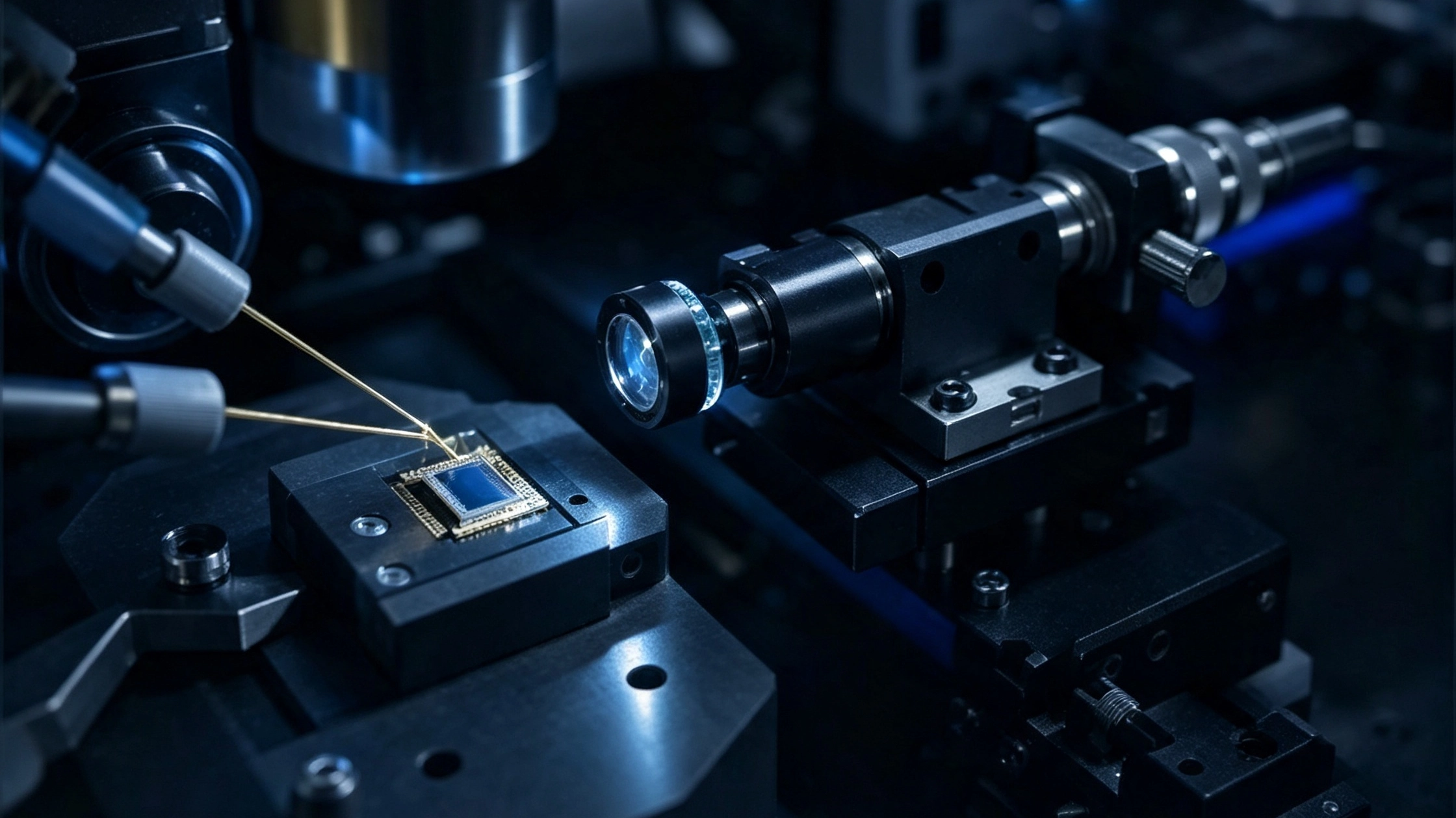
Wavelength matching
Start from the absorber, target, optical architecture or existing system—not from a generic part number.
Multiple power platforms
Portfolio options range from milliwatt‑class chips to high‑power 808 nm platforms, depending on wavelength.
Chip‑level customization
Renew die format, electrodes, facet requirements, operating mode and thermal interfaces around the application.
Qualification‑ready samples
Engineering samples allow optical, electrical, thermal and mechanical validation in the real system.
Connected manufacturing flow
Chip fabrication, facet processing, test and downstream integration are coordinated through one technical interface.
Prototype to volume
The qualified design becomes the baseline for follow‑on orders and controlled production scale‑up.
Precision light for demanding systems.
The portfolio is organized around how customers use the device—from trace‑gas detection and spectroscopy to ranging, medical and industrial systems.
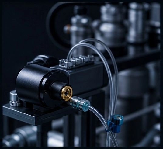
Gas Sensing & TDLAS
CH4 • CO • H₂O • process gases
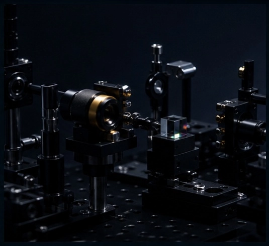
Spectroscopy
Atomic, molecular and laboratory analysis
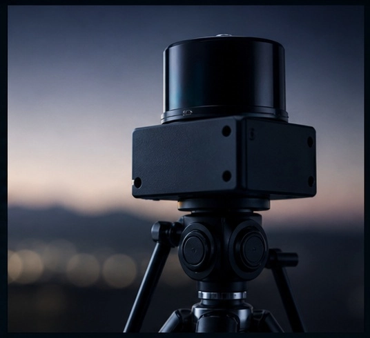
LiDAR & Rangelinding
905 nm and system‑level ranging solutions
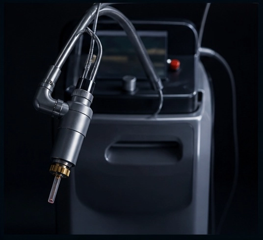
Medical & Aesthetic
808 / 1470 / 1940 /2100 nm platforms
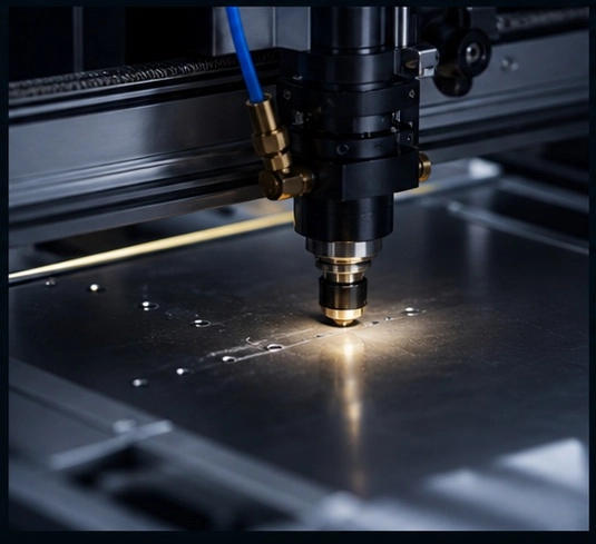
Industrial & Pumping
Laser pumping, marking and precision processing
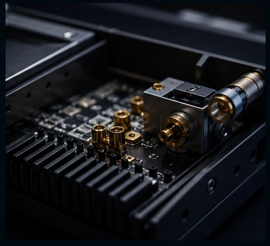
Research & OEM Integration
Custom light sources and photonics development